Table of Contents
System Description
Principle of Operation:
The basic principle of operation is to measure the current that flows in the antenna when it is excited by a constant voltage. In order to achieve simple high-performance current measurement, the excitation signal is used as the ground of the measurement circuitry. After conditioning and digitization, the signal is re-referenced to earth ground using opto-isolation.
There are five main parts of the system:
- The generator generates an 18 volt peak-to-peak pseudo-random signal and a floating 8 volt DC supply referenced to this signal which is used to power the measurement and antenna units.
- The antenna units which sense the capacitance using an antenna plate, transimpedance amplifier and gain stage/buffer.
- The measurement unit, which synchronously demodulates the antenna unit output, digitizes it and level-shifts it to the earth-ground reference. The measurement unit can acquire seven antenna inputs.
- The controller sequences the digitization, then decimates the signals 7x to 20.7 samples/sec. This data is then transmitted over a RS232 link to a Matlab application running on a PC.
- The host PC provides additional signal processing and display.
Generator:
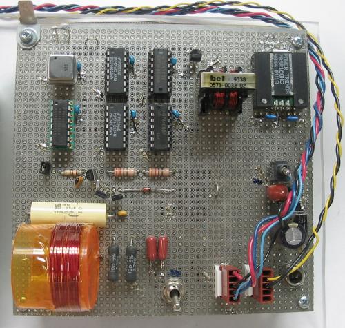
Since one generator can supply several measurement units and many antenna units, only one was needed for testing, so I used a hand-wired prototype:
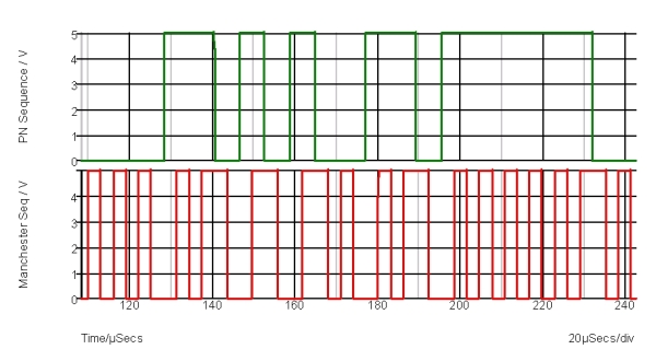
The pseudo-random noise generator is a top left. The pseudo-random signal is a 12 bit M-sequence with 10Hz repetition rate. Choosing a repetition rate that falls above the system bandwidth (1.5 Hz) insures that there are no low frequency components which can leak into the output.
The PN sequence is then Manchester encoded to shift the PN spectrum away from DC. By exclusive-or'ing with the clock, Manchester (or bi-phase) encoding turns the PN sequence which has long runs of zero and one bits into a sequence which only has runs of one or two bits:
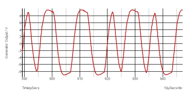
The half-bridge output stage is center left on the board, with the output coupling capacitor and filter below. A low-Q 2-pole RLC low-pass filter is used at the output to minimize RFI due to the PN sequence harmonics. The filtered output waveform looks like this (note different time scale):
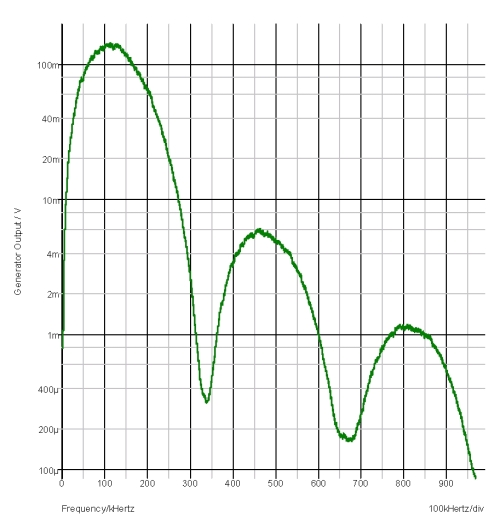
This is the generator output spectrum:
The right half of the generator board is power supply components. The entire capacitive sensor system operates off of 24 V DC supplied to the generator unit. A linear regulator drops this to 20 V for the output stage, and a switching regulator module generates 8 V DC for supplying the rest of the electronics. Since no dielectric isolation is required between the floating supply (referenced to the generator output) and the input power, and since there is no DC component in the output signal, isolation of the floating supply is done using a common-mode filter inductor, and no DC-DC converter is required.
Antenna Unit:
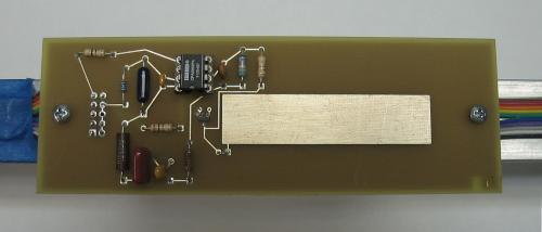
The antenna unit is constructed on a dual-sided PCB, the back side of which is dedicated to a ground plane. Since the measurement ground is the excitation signal, this plane serves as a guard which bootstraps the capacitance of the supporting structure, and also gives the sensor some degree of directionality. One of the characteristics of capacitive sensors is low directionality. This can be an advantage in close-in proximity sensing because objects cannot fall in a blind spot between the fields of view of adjacent sensors. The sensor plate is visible on the front of the board, and is 14 x 56 mm.
Signal conditioning electronics on the antenna unit function as a frequency selective current-to-voltage converter with transimpedance gain of 1 megohm (one volt per microamp.) A dual 40 MHz CMOS opamp is used to implement a transimpedance stage and a gain/buffer stage.
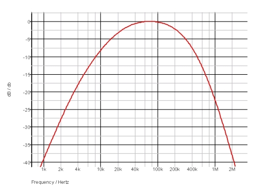
This is the receive frequency response, including the inherent single zero high-pass effect of the capacitive coupling:
The operating spectrum is centered on 80 kHz, with a 3 dB bandwidth of 200 kHz. The bandwidth is set using first-order RC sections, both for simplicity and also to give a stable frequency response. Due the broad spread spectrum of the excitation, a high-Q bandpass filter is not desirable. High Q filters would also contribute to phase and amplitude mismatch between the channels. The receive bandwidth is made wider than the transmit spectrum, also to limit the effect of filter drift on the received amplitude.
Four antenna units are connected to a 8 conductor mass-terminated IDC ribbon cable. Each sensor is “programmed” for its channel by removing 3 of the four possible output pins from the connector. The test antenna assembly has three antenna units mounted on an aluminum bar, which is also connected to the excitation signal:
The spacing between the antenna units is 60 cm.
Measurement Unit:
The functions of the measurement unit are: demodulation, phase/amplitude reference, digitization and level shifting. The measurement unit is constructed on a dual-sided PCB, with the back side largely dedicated to a ground plane/guard.
Note that this design has what I now consider to be a blunder in the demodulator. It effectively multiplies by the sequence:
{1, 0, 1, 0, ...}
instead of:
{1, -1, 1, -1, ...}
as is usually done in a synchronous demodulator. I knew I was doing this, but didn't understand that by going for this simpler design (using fewer switches) I was still rectifying the signal, but was sacrificing the demodulator's ability to reject low frequency interference. This is not as bad as it might be because the antenna unit has a highpass characteristic with 12 dB/octave rolloff.
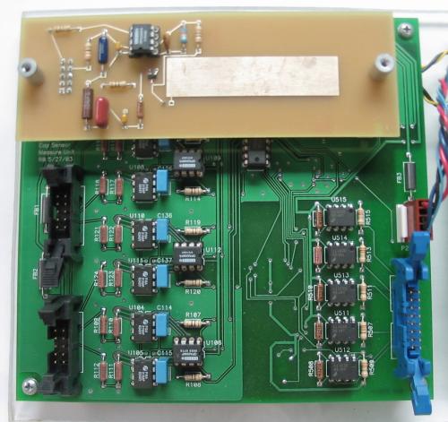
The daughter-board at top is the reference channel, which differs only from the active antenna units in that the input is connected to a capacitive divider rather than to the antenna patch. The capacitive divider and the reference clock generator are underneath the dummy antenna board. A comparator driven off of the reference channel output drives all of the demodulators, insuring the correct phase relationship between the excitation and the demodulator clock. The equivalent capacitance of the reference channel is 240 femto-Farads, which is near full scale. In later digital processing, the reference channel amplitude is used to normalize the other signals, resulting in ratiometric operation that is insensitive to variations such as changes in the generator level or ADC reference.
Five of the eight demodulator sections are visible on the left, next to the connectors for two antenna unit strings. There are only seven sensor channels because one of the demodulators is used for the reference channel. The synchronous demodulator is implemented using a CMOS switch, with an RC combination used to reconstruct the level, giving a 2.5 Hz -3dB point.
The demodulator outputs are multiplexed, then digitized using a 24 bit sigma-delta ADC. Each channel is sampled at 145 samples/sec. The oversampling allows later digital filtration to improve the selectivity. The sampling rate is chosen so that the first few 60 Hz harmonics do not fall in aliases of the system passband, further improving rejection of power line harmonics. The ADC is mounted on the underside of the board, as are other SMT components such as decoupling capacitors.
At the lower right is the opto-isolation section which converts from the floating ground (the excitation signal) to the earth referenced ground used at the output. The large blue right side connector goes to the controller card, and the small connector goes to the generator. A 5 volt regulator is also hidden by the reference channel board.
Assembly with Controller:
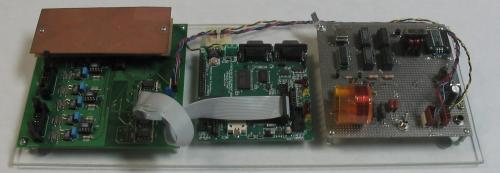
This image shows the complete assembly of all the electronics, excluding the antennas:
The controller board is in the center. The reference channel card on the measurement unit is covered with a shield panel to eliminate residual capacitance sensitivity. Other than this, the system operates without any shielding, despite the location of picoamp/microvolt sensitive circuits near power and digital electronics.
A commercial AVR 8-bit microcontroller development board was used as the controller. Only the microcontroller itself and the RS232 interface are used, and in a production version, it would make sense to place the controller chip on the measurement unit and do level shifting at the serial or network interface.
In addition to sequencing the ADC and multiplexer on the measurement unit, the controller also decimates the the ADC data using a 6'th order butterworth IIR filter with cutoff set at 4 Hz. The data output rate is 145/7 samples/sec (about 21 samples/sec.)
Host PC:
In additional to collection and display of experimental data, the host PC does some signal processing. A 1.5 Hz low-pass FIR filter is used to establish the final system bandwidth. The system bandwidth is a tradeoff between response time and noise rejection. The bandwidth was chosen to be as narrow as possible while still giving a response time of about 1/2 second.
The host PC also subtracts out the background capacitance to allow the influence of objects to be easily seen. Background subtraction is done by taking the minimum reading in a time window and using that as the zero value.
My electronics page | Up | Prev | Next | email

